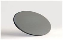
Germanium wafer
Germanium wafer is an excellent semiconductor material and widely used in variety applications such as Sensor, Solar cell, Infrared optics applications, high brightness LEDs, and various semiconductor applications.
| Growth | CZ or VGF | ||||||
| Diameter | 100 ± 0.4 | 150 ± 0.5 | mm | ||||
| Thickness | 175 ± 25 | 250 ± 25 | |||||
| Type | N or P | ||||||
| Orientation | (100) 6˚ or 9˚ toward (111) ± 0.5 | degree | |||||
| Primary Flat Orientation | (100) ± 0.5 | degree | |||||
| Length | 32.5 ± 2.5 | 57.5 ± 2.5 | mm | ||||
| Secondary Flat Orientation | None | ||||||
| Resistivity | 0.001 - 20 | Ω.cm | |||||
| Mobility | (0.25 - 1.5) X 103 | cm2/v.s | |||||
| Carrier Concentration | (0.5 - 30) X 1017 | ea/cm-3 | |||||
| Etch Pit Density | ≦ 2000 | ea/cm-2 | |||||
| Front Side Surface | Epi ready Polished | ||||||
| Back Side Surface | Etch | ||||||
| Edge Profile | Round | ||||||