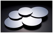
InP wafer
InP is commonly used in high-power and high-frequency electronics devices because of its superior electron velocity characteristics. It also has a direct bandgap, making it useful for optoelectronics devices like laser diodes. InP is also used as a substrate for epitaxial InGaAs based opto-electronic devices.
|
Product Name |
InP Wafer |
Unit |
||
|
Diameter |
50.8 ~ 100 |
mm |
||
|
Orientation* |
(100) ± 0.5° |
degree |
||
|
Thickness* |
(350~625) ± 25 |
µm |
||
|
Type/Dopant |
N / S or Sn |
P / Zn |
N / Undoped |
|
|
Carrier Concentration |
(0.8-8) x 1018 |
(1-10) x 1015 |
cm-3 |
|
|
Mobility |
(1-2.5) x 103 |
50 ~ 100 |
(3-5) x 103 |
cm2/Vs |
|
Etch Pitch Density |
100 ~ 5000 |
≤ 500 |
≤ 5000 |
cm2 |
|
TTV* |
SSP : ≤ 15 , DSP : ≤ 10 |
µm |
||
|
Warp |
≤ 15 |
µm |
||
|
Surface |
Etched or Polished |
|
||
|
* Other customized specifications are welcome |
||||