LN/ LT wafer (Lithium Niobate/ LithumTantalate)
LN Wafer (LiNbO3)
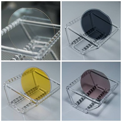
LN wafer is an ideal material for versatile applications in the fields of photonics and optoelectronics such as Detectors, Sensors, Phased-array radar and Electro-optic modulators..etc. The single crystal LN thin films will be used for developing wide-bandwidth, high speed and high efficiency electronic devices and photonic circuits.
|
Product Name
|
Lithium Niobate LiNbO3 (LN) Wafer
LithumTantalate LiTaO3 (LT) Wafer
|
Unit
|
||
|
Diameter
|
76.2
|
100
|
150
|
mm
|
|
Orientation
|
LN: 64° Rot. Y-cut±0.2° / 127.86° Rot. Y-cut±0.2° / Y-cut±0.2
LT:36° Rot. Y-cut±0.2° / 42° Rot. Y-cut±0.2° / X-cut±0.2°
|
degree
|
||
|
Primary Flat
|
LN: Perpendicular to X ± 0.2° / Perpendicular to Z±0.2°
Perpendicular to X ± 0.2° / Perpendicular to 112.2° Y±0.2°
|
degree
|
||
|
Secondary Flat
|
LN: CW 180° / CW 225° / CW 270°±0.5° from Primary
LT: CW 225° / CW 270° / CW 315°±0.5° from Primary
|
degree
|
||
|
Thickness*
|
(200~500) ± 20
|
μm
|
||
|
TTV
|
≤ 10
|
μm
|
||
|
Bow
|
≤ 25
|
μm
|
||
|
Front Surface
|
Ra ≤ 8
|
Å
|
||
|
Back Surface
|
LN: 0.2 ≤ Ra ≤ 0.7
LT:0.2 ≤ Ra ≤ 0.5 or 0.08 ≤ Ra ≤ 0.15
|
μm
|
||
|
Edge Beveling
|
Rounded
|
|
||
|
Curie Temp.
|
LN: 1142 ± 3
LT:605 ± 3
|
̊C
|
||
|
* Other surface conditions & customized specifications are welcome
* Blackening or Non-Blackening is also available
|
||||