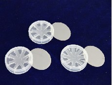
GaN-FS wafer
Free standing GaN (Gallium Nitride) substrate wafer is mainly used for UHB-LED and LD application. The well-known effect of using free-standing GaN substrates can be improved material quality, reducing parasitic resistance effects for creating nitride semiconductor devices.
|
Product Name |
GaN-FS |
|
||||
|
Diameter |
50.8 ± 1.0 |
100 mm ± 0.1 |
mm |
|||
|
Type/Dopant |
N / Ge or Si |
N / Undoped |
SI / Fe or Carbon |
N / Undoped |
N / Si |
|
|
Resistivity |
< 0.05 |
< 0.5 |
>106 |
< 0.5 |
< 0.05 |
Ω.cm |
|
Orientation* |
C-plane (0001) off toward M-Axis 0.35°± 0.15° |
C-plane(0001) ± 0.5° |
degree |
|||
|
Thickness* |
350~500 ± 25 |
µm |
||||
|
Dislocation Density |
(0.5~3) x 106 |
(0.1~3) x 106 |
(0.1~3) x 106 |
>5 x 10⁶ |
cm-2 |
|
|
Front Surface |
Polished (Ra<0.2nm) |
|
||||
|
Back Surface |
Fine ground |
|
||||
|
Useable Surface Area |
> 90 |
% |
||||
|
* Other conditions & customized specifications are welcome |
||||||