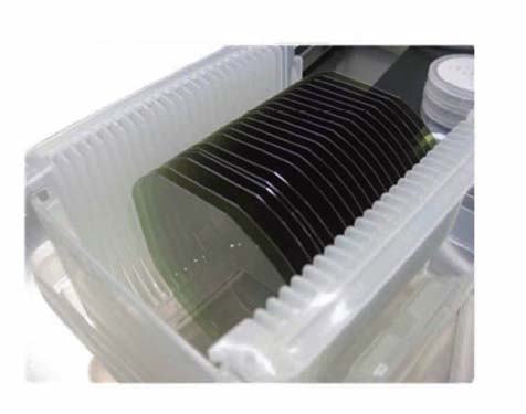
SiC Epi
SiC EPI wafers are used in producing Schottky diodes, MOSFETs, JFETs, and BJTs over a wide voltage range and customized wafers for thyristors, GTOs and IGBTs over a wider voltage range for medium to very high voltage power conversion system applications.
|
Product Name
|
SiC / SiC Wafer
|
Unit
|
|
|
Diameter
|
50.8 ~ 150
|
mm
|
|
|
Conductivity
|
N - Type
|
P -Type
|
|
|
Dopant
|
Nitrogen
|
Aluminum
|
|
|
Carrier Concentration
|
9 x 10¹⁴ ~ 1 x 10¹⁹
|
9 x 10¹⁴ ~ 1 x 10¹⁹
|
cm-3
|
|
Tolerance
|
± 15
|
± 50
|
%
|
|
Uniformity
|
≤ 10
|
≤ 20
|
%
|
|
Thickness*
|
0.2 ~ 50
|
µm
|
|
|
Tolerance
|
± 10
|
%
|
|
|
Uniformity
|
≤ 10
|
%
|
|
|
Defects
|
< 1
|
cm-2
|
|
|
Roughness (20µmX20µm)
|
≤ 0.5
|
nm
|
|
|
Scratches
|
<1 x wafer diameter
|
ea/mm
|
|
|
Usable Area
|
≥90
|
%
|
|
|
* Other customized specifications are welcome
|
|||