GaN Epitaxial Wafer
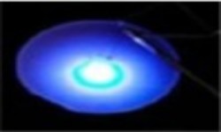
GaN light-emitting diode (LED) epitaxial structure was grown on the sapphire wafer with the pyramidal pattern and the standard flat sapphire wafer. It is used for ultra high brightness blue and green light emitting diodes (LED) and laser diodes (LD) application.
|
GaN Blue LED EPI Wafer Spec |
||||||
|
Spec |
||||||
|
EPI Wafer Size |
||||||
|
Growth |
MOCVD |
|||||
|
Diameter |
50.8 ± 0.2 mm |
|||||
|
Thickness |
430 ± 30 um |
|||||
|
EPI thickness |
8 ± 3 um |
|||||
|
Surface ontact dopant |
Mg / Zn / C / SiP |
|||||
|
Edge exclusion |
3 mm |
|||||
|
EPI Wafer Structure |
||||||
|
P |
GaN |
|||||
|
P |
AlGaN |
|||||
|
Active area |
InGaN / GaN |
|||||
|
N |
GaN |
|||||
|
U |
GaN |
|||||
|
Substrate |
Sapphire |
|||||
|
EPI Wafer Parameter |
||||||
|
Item |
Unit |
Blue |
Description |
|||
|
Wave Length (λD) |
nm |
430 ~ 480 |
IF =20mA |
|||
|
VF |
V |
< 3.4 |
Forward Voltage |
|||
|
Based on Chip Size |
10 x 23 mil |
6 x 9 mil |
|
|||
|
(Iv) |
Mcd |
A |
0 – 10 |
A |
0 – 10 |
IF =20mA |
|
B |
10 – 20 |
B |
10 – 13 |
|||
|
C |
20 – 23 |
C |
13 – 14 |
|||
|
D |
23 – 24 |
D |
14 – 15 |
|||
|
E |
24 – 25 |
E |
15 – 16 |
|||
|
F |
25 – 26 |
F |
16 – 17 |
|||
|
G |
26 – 27 |
G |
17 – 18 |
|||
|
H |
27 – 28 |
H |
> 18 |
|||
|
I |
> 28 |
|
|
|||
|
Notes: |
||||||
|
l Wave Length and Luminous intensity can be change by customer request. |
||||||
|
l Luminous intensity data is base on the chip size test result that made from ATECOM’s EPI Wafer |
||||||