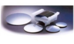
GaAs Wafer
GaAs is a compound semiconductor material which is made by arsenic and gallium, is a kind of the electronic information material with excellent performance. It is the most widely used in mobile communication, satellite communication, semiconductor lighting (LED) radar and infrared detection, efficient solar cells and laser diode (LD).
|
Product Name
|
GaAs Wafer
|
|
||
|
Diameter
|
50.8 ~ 150
|
mm
|
||
|
Dopant
|
N / Si
|
P / Zn
|
SI / Carbon
|
|
|
Thickness*
|
(350 ~ 675) ± 25
|
μm
|
||
|
Surface Orientation*
|
On-axis : (100) ± 0.5º
Off-axis:2º / 6º /15º off toward<111> ± 0.5º |
degree
|
||
|
Hall Mobility*
|
≥1000 ~ 2500
|
≥50 ~ 120
|
≥4000~5000
|
cm2/V.S
|
|
Etch Pit Density*
|
≤100 ~ 5000
|
≤ 3000 ~ 5000
|
≤ 1500 ~ 5000
|
cm-2
|
|
Carrier Concentration*
|
(0.8 ~ 4.0) x 1018
|
(0.5 ~ 5.0) x 1019
|
≤ 1 x 10⁸
|
cm-3
|
|
TTV(DSP)*
|
≤ 4
|
μm
|
||
|
TTV(SSP)*
|
≤ 10
|
μm
|
||
|
Warp*
|
≤ 15
|
μm
|
||
|
Front Side / Back Side
|
Etched or Polished
|
|
||
|
* Other surface conditions & customized specifications are welcome
|
||||